Exploring the Printed Circuit Board The Organized Foundation of Electronic Systems
The printed circuit board (PCB) is one of the most fundamental yet often overlooked components in electronics. Found inside almost every electronic product—ranging from basic household appliances to sophisticated satellites—a PCB acts as the central organizing structure that holds components in place and provides the electrical pathways necessary for them to communicate. Without this technology, modern devices would be larger, less reliable, and far more expensive to produce.
This in-depth educational guide examines what a PCB is, why it exists, how it is structured, the range of forms it can take, the materials and processes involved in its creation, and its critical role across industries. Presented in a neutral, factual manner and based on established engineering principles and industry standards, the article aims to provide a distinctive perspective by emphasizing the PCB’s role as an enabler of systematic complexity in an increasingly connected world.
The Problem It Solved: Moving Beyond Chaotic Wiring
In the early days of electronics, circuits were constructed by hand-soldering wires directly between component leads and terminals. This point-to-point method worked for simple vacuum-tube radios but quickly became impractical as circuits grew more intricate. Wiring errors were common, repairs were difficult, and consistent mass production was nearly impossible.
The PCB emerged as an elegant solution: a flat insulating board with predefined conductive patterns that replace individual wires. By standardizing interconnections, it allowed engineers to design complex systems with confidence that they could be reliably reproduced. The transition from wired assemblies to printed boards marked a pivotal shift, comparable to moving from handwritten manuscripts to the printing press in terms of scalability and consistency.
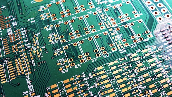
Basic Anatomy of a PCB
A typical PCB consists of several key elements working together:
- Substrate: A rigid or flexible insulating base that provides mechanical strength.
- Conductive layers: Thin copper foil bonded to the substrate and patterned into traces (narrow paths), pads (connection points for components), and larger planes (for power or ground distribution).
- Vias: Plated holes that carry signals between layers in multi-layer designs.
- Solder mask: A protective polymer layer, usually green, that covers traces while leaving pads exposed for soldering.
- Legend (silkscreen): Printed text and symbols indicating component locations and orientations.
When components are soldered onto the pads, electrical current flows through the copper traces in a controlled, predictable manner. This organized layout minimizes parasitic effects such as capacitance and inductance that plagued early wired circuits.
Evolution Through the Decades
Although ideas for printed wiring date to the 1920s, practical PCBs gained traction during World War II for military equipment requiring compactness and reliability. Post-war commercialization began in earnest in the 1950s with single-sided phenolic boards used in radios and televisions.
Key milestones include:
- Late 1950s: Plated-through holes enabled reliable double-sided boards.
- 1960s–1970s: Multi-layer boards and automated drilling improved density and signal quality.
- 1980s: Surface-mount technology (SMT) replaced most through-hole components, shrinking board sizes dramatically.
- 1990s–2000s: High-density interconnect (HDI) with microvias supported the mobile phone revolution.
- 2010s–present: Flexible, rigid-flex, and advanced thermal materials address wearables, automotive electrification, and 5G/6G infrastructure.
Each advancement responded to new demands for smaller size, higher speed, greater power handling, or improved environmental resilience.
Types and Configurations
PCBs are engineered in various architectures to match application requirements:
- Single-sided: Copper on one side only. Cost-effective for low-density circuits such as LED drivers or simple sensors.
- Double-sided: Copper on both sides with plated-through vias. Standard for many consumer and industrial products.
- Multi-layer: Four to over sixty layers, with internal planes dedicated to power and ground. Essential for high-speed digital systems where controlled impedance and low noise are critical.
- Flexible: Built on polyimide or polyester films that bend repeatedly without damage. Used where space is limit or movement occurs.
- Rigid-flex: Integrates rigid multi-layer sections with flexible tails in one cohesive board, reducing connectors and improving reliability in dynamic environments.
- HDI (High-Density Interconnect): Employs microvias, blind/buried vias, and very fine traces to pack more functionality into less area—dominant in smartphones and advanced medical devices.
Specialized variants include metal-core boards for efficient heat spreading in high-power lighting and high-frequency laminates for microwave and millimeter-wave circuits.
Materials Science Behind the Board
Material choices balance electrical, thermal, mechanical, and economic factors:
- FR-4 epoxy-glass laminate remains the workhorse due to its flame retardance, mechanical stability, and moderate cost. Higher-Tg versions withstand modern lead-free soldering temperatures.
- Polyimide excels in flexible circuits for its outstanding thermal and chemical resistance.
- PTFE or ceramic-filled hydrocarbons provide low dielectric loss for RF and high-speed digital signals.
- Copper foil thickness is select base on current load and impedance needs.
- Surface finishes such as ENIG, immersion silver, or OSP protect pads and ensure reliable soldering over time.
Global regulations including RoHS and REACH have largely eliminated lead and certain hazardous substances, pushing the industry toward greener alternatives without sacrificing performance.
From Design to Finished Board: The Production Sequence
Fabrication is a precise, multi-step process governed by IPC standards:
- Layout design in EDA software, incorporating design-for-manufacturability rules.
- Pattern imaging via photoresist and UV exposure or laser direct imaging.
- Etching to remove unwanted copper.
- Drilling or laser ablation for vias.
- Copper plating of holes and surfaces.
- Layer alignment and lamination under controlled heat and pressure (multi-layer).
- Solder mask application and curing.
- Silkscreen printing.
- Surface finish deposition.
- Electrical testing and inspection (flying probe, AOI, X-ray for inner layers).
Component assembly follows as a separate stage involving stencil printing of solder paste, automated placement, reflow soldering, and final functional testing.
Why PCBs Enable Modern Innovation
The PCB’s greatest contribution is transforming electronics from craft to engineering discipline. By providing a repeatable interconnection platform, it allows designers to focus on system-level functionality rather than individual connections. This standardization has:
- Reduced device size by orders of magnitude
- Lowered production costs through automation
- Improved reliability via controlled manufacturing
- Accelerated innovation cycles
Applications span every sector: consumer gadgets, automotive safety systems, medical diagnostics, aerospace avionics, telecommunications networks, renewable energy converters, and industrial automation.
Current Landscape and Emerging Trends (Late 2025)
Demand continues to grow with electric vehicles, AI hardware, and IoT proliferation. Notable developments include:
- Advanced HDI and substrate-like Printed Circuit Board for ever-finer integration
- Wider adoption of rigid-flex in foldable devices and compact medical tools
- Embedded components to further reduce footprint
- Materials with enhanced thermal conductivity for high-power applications
- Sustainable substrates and processes aligned with circular-economy goals
- Increased use of AI-assisted design and automated optical inspection
These directions ensure PCBs will support the next wave of technological advancement.
Closing Perspective
A printed circuit board—commonly called a pcb board—is far more than a simple carrier of components. It is a meticulously engineered platform that imposes order on electrical complexity, enabling the sophisticated, reliable, and affordable devices that define contemporary life.
Understanding the principles behind PCBs provides deeper appreciation for the engineering that quietly underpins the digital age. As new challenges arise in speed, power density, flexibility, and sustainability, the PCB will continue adapting, remaining an indispensable foundation for electronic innovation well into the future.
Disclaimer
This article is intended for informational and educational purposes only. The content provided is based on general engineering principles, publicly available industry knowledge, and commonly accepted standards related to printed circuit board (PCB) design, materials, and manufacturing. It does not constitute professional engineering advice, technical certification, or a substitute for consultation with qualified electronics engineers, manufacturers, or regulatory authorities.
While every effort has been made to ensure accuracy and clarity, technologies, standards, materials, and regulations in the electronics industry may change over time. The author and publisher make no representations or warranties regarding the completeness, accuracy, or suitability of the information for any specific application. Any reliance placed on this information is strictly at the reader’s own risk.